- 您现在的位置:买卖IC网 > Sheet目录1207 > DAK-14A (Power Integrations)KIT DESIGN ACCELERATOR ADAPTER
�� �
�
�TNY263-268�
�Key� Application� Considerations�
�TinySwitch-II� vs.� TinySwitch�
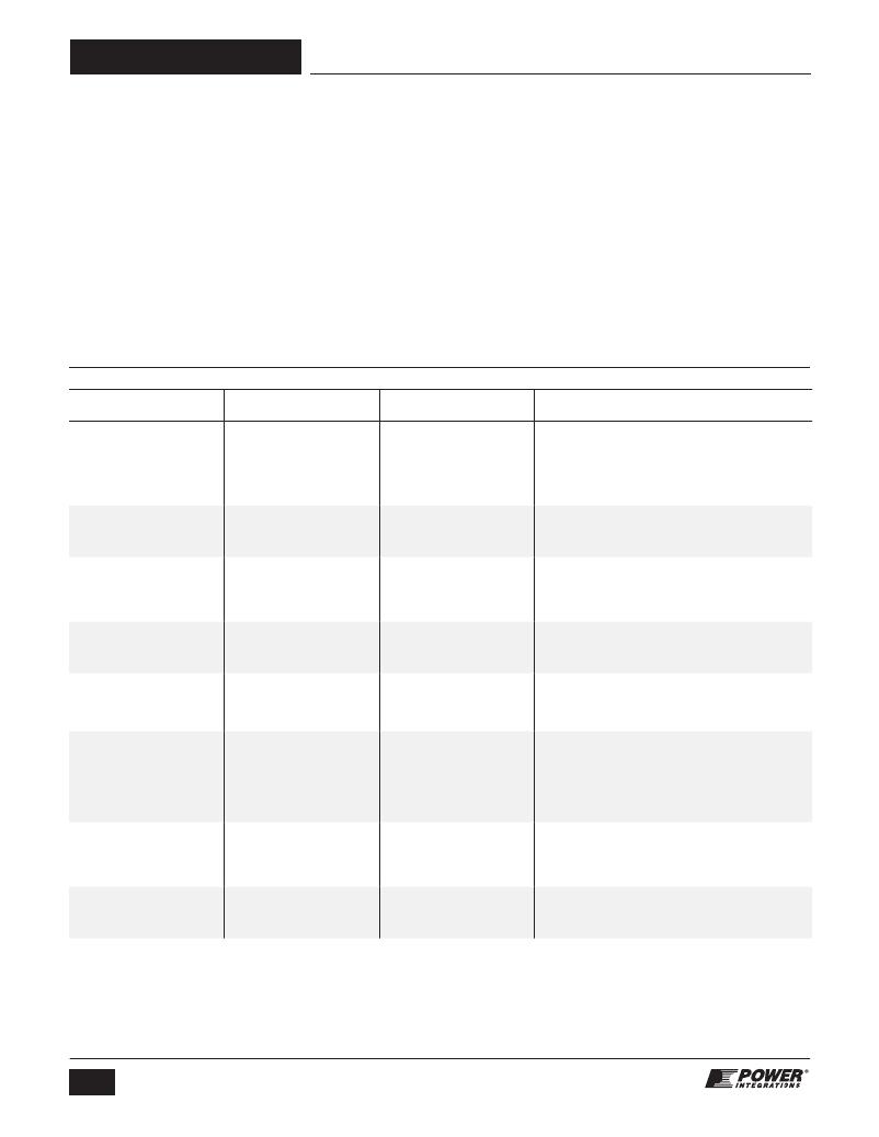
�Table� 2� compares� the� features� and� performance� differences�
�between� the� TNY254� device� of� the� TinySwitch-II� family� with�
�the� TinySwitch-II� family� of� devices.� Many� of� the� new� features�
�eliminate� the� need� for� or� reduce� the� cost� of� circuit� components.�
�Other� features� simplify� the� design� and� enhance� performance.�
�Design�
�Output� Power�
�Table� 1� (front� page)� shows� the� practical� continuous� output�
�power� levels� that� can� be� obtained� under� the� following�
�conditions:�
�TinySwitch-II� vs.� TinySwitch�
�1.� The� minimum� DC� input� voltage� is� 90� V� or� higher� for�
�85� VAC� input,� or� 240� V� or� higher� for� 230� VAC� input� or�
�115� VAC� input� with� a� voltage� doubler.� This� corresponds� to�
�a� ?lter� capacitor� of� 3� μ� F/W� for� universal� input� and� 1� μ� F/W�
�for� 230� VAC� or� 115� VAC� with� doubler� input.�
�2.� A� secondary� output� of� 5� V� with� a� Schottky� recti?er� diode.�
�3.� Assumed� ef?ciency� of� 77%� (TNY267� &� TNY268),� 75%�
�(TNY265� &� TNY266)� and� 73%� (TNY263� &� TNY264).�
�4.� The� parts� are� board� mounted� with� SOURCE� pins� soldered�
�to� suf?cient� area� of� copper� to� keep� the� die� temperature� at�
�or� below� 100� °� C.�
�In� addition� to� the� thermal� environment� (sealed� enclosure,�
�ventilated,� open� frame,� etc.),� the� maximum� power� capability� of�
�TinySwitch-II� in� a� given� application� depends� on� transformer�
�Function�
�TinySwitch�
�TNY254�
�TinySwitch-II�
�TNY263-268�
�TinySwitch-II�
�Advantages�
�Switching� Frequency� and�
�Tolerance�
�Temperature� Variation�
�(0-100� °� C)**�
�44� kHz� ±10%� (at� 25� °� C)�
�+8%�
�132� kHz� ±6%� (at� 25� °� C)�
�+2%)�
�?�
�?�
�?�
�?�
�Smaller� transformer� for� low� cost�
�Ease� of� design�
�Manufacturability�
�Optimum� design� for� lower� cost�
�Active� Frequency� Jitter�
�N/A*�
�±4� kHz�
�?� Lower� EMI� minimizing� ?lter�
�component� costs�
�Transformer� Audible� Noise�
�Reduction�
�N/A*�
�Yes–built� into� controller�
�?� Practically� eliminates� audible� noise� with� ordinary� dip�
�varnished� transformer� –� no� special�
�construction� or� gluing� required�
�Line� UV� Detect�
�N/A*�
�Single� resistor�
�?� Prevents� power� on/off� glitches�
�programmable�
�Current� Limit� Tolerance�
�Temperature� Variation�
�(0-100� °� C)**�
�Auto-Restart�
�±11%� (at� 25� °� C)�
�-8%�
�N/A*�
�±7%� (at� 25� °� C)�
�0%)�
�6%� effective� on-time�
�?� Increases� power� capability� and�
�simpli?es� design� for� high� volume�
�manufacturing�
�?� Limits� output� short-circuit� current� to� less� than� full�
�load� current�
�?� No� output� diode� size� penalty�
�?� Protects� load� in� open� loop� fault� conditions�
�?� No� additional� components� required�
�BYPASS� Pin� Zener� Clamp�
�N/A*�
�Internally� clamped� to� 6.3� V�
�?� Allows� TinySwitch-II� to� be� powered� from� a� low�
�voltage� bias� winding� to� improve� ef?ciency� and� to�
�reduce� on-chip� power� dissipation�
�DRAIN� Creepage� at� Package�
�0.037� in.� /� 0.94� mm�
�0.137� in.� /� 3.48� mm�
�?� Greater� immunity� to� arcing� as� a� result� of� dust,�
�debris� or� other� contaminants� build-up�
�*Not� available.�
�**� See� typical� performance� curves.�
�Table� 2.�
�10�
�Rev.� H� 02/09�
�Comparison� Between� TinySwitch� and� TinySwitch-II.�
�www.powerint.com�
�发布紧急采购,3分钟左右您将得到回复。
相关PDF资料
DAK-91
DESIGN ACCELERATOR KIT III SWTCH
DAL3W3P300G30LF
CONN DSUB PLUG 3W3 T/H GOLD
DAL3W3S300G30LF
CONN DSUB RCPT 3W3 T/H GOLD
DAL7W2P300G30LF
CONN DSUB PLUG 7W2 T/H GOLD
DAL7W2P300G40LF
CONN DSUB PLUG 7W2 T/H GOLD
DAL7W2P500G30LF
CONN DSUB PLUG 7W2 T/H RA GOLD
DAL7W2S500G30LF
CONN DSUB RCPT 7W2 T/H R/A GOLD
DAL7W2SA00LF
DSUB POWER STB 7W2 SOCK
相关代理商/技术参数
DAK1575MS50T
制造商:TOKO 制造商全称:TOKO, Inc 功能描述:GPS DIELECTRIC PATCH ANTENNA
DAK159
制造商:Amphenol Corporation 功能描述:DAK159 - Bulk
DAK-15P
制造商:ITT Interconnect Solutions 功能描述:DAK-15P - Bulk
DAK15PF179
制造商:ITT 功能描述:DSUB 15 M WW2 G ZINC
DAK-15P-F179
制造商:ITT Interconnect Solutions 功能描述:DAK-15P-F179 - Bulk
DAK15PF179A
制造商:ITT 功能描述:DSUB 15 M SOD .154 MH WW ZINC
DAK15S
制造商:ITT 功能描述:DSUB 15 F SOD G ZINC 制造商:ITT Interconnect Solutions 功能描述:DSUB 15 F SOD G ZINC
DAK-15S
制造商:ITT Interconnect Solutions 功能描述:DAK-15S - Bulk